|
1.5MHz高效单片同步降压调节器CXSD62130电流模式方案100%占空比从2.7V到6.0V的输入 | ||||||||||||||||||||||||||||||||||||||||||||||||||||||||||||||||||||||||||||||||||||||||||||||||||||||||||||||||||||||||||||||||||||||||||||||||||||||||||||||||||||||||||||||||||||||||||||||||||||||||||||||||||||||||||||||||||||||||||||||||||||||||||||
|
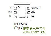
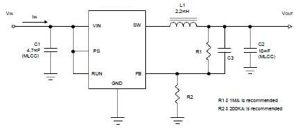
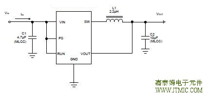
目录 1.产品概述 2.产品特点 一,产品概述(General Description) CXSD62130 CXSD62130A is a 1.5MHz high efficiency monolithic synchronous buck regulator. Design with current mode scheme,the CXSD62130 CXSD62130A is stable with ceramic output capacitor. Input voltage from 2.7V to 6.0V makes the CXSD62130 CXSD62130A ideally suited for single Li-Ion battery powered applications. 100%duty cycle provides low dropout operation, extending battery life in portable electrical devices. Theinternally fixed 1.5MHz operating frequency allows the using of small surface mount inductors and capacitors. The synchronous switches included inside increase the efficiency and eliminate the need of an external Schottky diode. 1A Output Current HD STB 需要详细的PDF规格书请扫一扫微信联系我们,还可以获得免费样品以及技术支持! 五,产品封装图 (Package)
七,功能概述 Main Control Loop switching regulato r. In normal operation, the internal P-channel power MOSFET is turned on each cycle. The peak inductor current at which ICMP turn off the P-FET is controlled by the voltage on the COMP node, which is the output of the error amplifier (EAMP). An external resistive divider connected between VOUT and ground allows the EAMP to receive an output feedback voltage VFB at FB pin. When the load current increases, it causes a slightly decrease in VFB relative to the 0.6V reference, which in turn causes the COMP voltage to increase until the average inductor current matches the new load current. in shutdown, the internal power MOSFETs turn off, all internal circuitry shuts down and the quiescent supply current reduces to 0.5μA maximum. converter. At light loads, the CXSD62130 CXSD62130A will automatically enter in pulse frequency mode operation to reduce the dominant switching losses. In PFM operation, the inductor current may reach zero or reverse on each pulse. A zero current comparator turn off the N-FET, forcing DCM operation at light load. These controls get very low quiescent current, help to maintain high effi-ciency over the complete load range. prevent sub-harmonic oscillations, theCXSD62130 CXSD62130A sense the peak current and add slope compensation to stable the converter. It is accomplished in-ternally by adding a compensating ramp to the inductor current signal at duty cycles in excess of 40%. Normally,this results in a reduction of maximum inductor peak current for duty cycles > 40%. However, the CXSD62130 CXSD62130A uses a special scheme that counteracts this compensating ramp, which allows the maximum inductor peak current to remain unaffected throughout all duty cycles. cycle increases toward the maximum on time. Further, reduction of thesupply voltage forces the main switch to remain on for more than one cycle until it reaches 100% duty cycle. The input voltage minus the voltage drop will determine the output voltage across the P-FET and the inductor.An important detail to remember is that on resistance of P-FET switch will increase at low input supply voltageTherefore, the user should calculate the power dissipa- When the junction temperature ex-ceeds 150oC, a thermal sensor turns off the both power MOSFETs, allowing the devices to cool. The thermal sen-sor allows the converters to start a soft-start process and regulate the output voltage again after the junction tem-perature cools by 30oC. The OTP is designed with a 30oC hysteresis to lower the average Junction Temperature (TJ) during continuous thermal overload conditions, in-creasing the lifetime of the device.
发表评论
| ||||||||||||||||||||||||||||||||||||||||||||||||||||||||||||||||||||||||||||||||||||||||||||||||||||||||||||||||||||||||||||||||||||||||||||||||||||||||||||||||||||||||||||||||||||||||||||||||||||||||||||||||||||||||||||||||||||||||||||||||||||||||||||
发表时间:2020-04-25浏览次数:311
| 最新信息 |
|---|
| (1.)CXLE86296D 五通道高 ... (2.)CXLE86295D 五通道高 ... (3.)CXLE86294E PWM调光LE ... (4.)CXLE86293EI 线性恒流 ... (5.)CXLE86292CI 五通道I2 ... (6.)CXLE86291C 三通道PWM ... (7.)CXLE83205X PWM调光LE ... (8.)CXLE83204XS高精度PWM ... (9.)CXLE83203F:高功率DIP7 ... (10.)CXLE83202F:高精度PWM ... |
| 头条信息 |
|---|


