|
CXSD6297电压模式固定300kHz开关频率同步降压变换器上电复位(POR)电路监测VCC电源电压以防止错误的逻辑控制 | ||||||||||||||||||||||||||||||||||||||||||||||||||||||||||||||||||||||||||||||||||||||||||||||||||||||||||||||||||||||||||||||||||||||||||||||||||||||||||||||||||||||||||||||||||||||||||||||||||||||||||||||||||||||||||||||||||||||||||||
|
目录 1.产品概述 2.产品特点 一,产品概述(General Description) The CXSD6297 is a voltage mode, fixed 300kHz switching frequency, synchronous buck converter. The CXSD6297 allows wide input voltage that is either a single 5V~12V or two supply voltage(s) for various applications. The power-on-reset (POR) circuit monitors the VCC supply voltage to prevent wrong logic controls. A built-in soft-start circuit prevents the output voltages from overshoot as well as limits the input current. An internal 0.8V tempera-ture-compensated reference voltage with high accuracy is designed to meet the requirement of low output volt-age applications. The CXSD6297 provides excellent out-put voltage regulations against load current variation.CXSD6297 is built in reference voltage offset function for applications that require adjusting supply voltage.The controller’s over-current protection monitors the out-put current by using the voltage drop across the RDS(ON) of low-side MOSFET, eliminating the need for a current sens-ing resistor that features high efficiency and low cost. In addition, the CXSD6297 also integrates excellent protec-tion functions, The over-voltage protection (OVP) , under-voltage protection (UVP) and over-temperature protec-tion (OTP). OVP circuit which monitors the FB voltage to prevent the PWM output from over voltage, and UVP cir-cuit which monitors the FB voltage to prevent the PWM output from under voltage or short circuit. OTP circuit which 1.)Wide 5V to 12V Supply Voltage Graphic Cards 需要详细的PDF规格书请扫一扫微信联系我们,还可以获得免费样品以及技术支持!
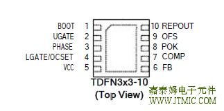
五,产品封装图 (Package)
六.电路原理图
七,功能概述 Layout Consideration 八,相关产品 更多同类产品......
发表评论
| ||||||||||||||||||||||||||||||||||||||||||||||||||||||||||||||||||||||||||||||||||||||||||||||||||||||||||||||||||||||||||||||||||||||||||||||||||||||||||||||||||||||||||||||||||||||||||||||||||||||||||||||||||||||||||||||||||||||||||||
发表时间:2020-04-22浏览次数:331


| 最新信息 |
|---|
| (1.)CXLE86296D 五通道高 ... (2.)CXLE86295D 五通道高 ... (3.)CXLE86294E PWM调光LE ... (4.)CXLE86293EI 线性恒流 ... (5.)CXLE86292CI 五通道I2 ... (6.)CXLE86291C 三通道PWM ... (7.)CXLE83205X PWM调光LE ... (8.)CXLE83204XS高精度PWM ... (9.)CXLE83203F:高功率DIP7 ... (10.)CXLE83202F:高精度PWM ... |
| 头条信息 |
|---|

