|
脉冲宽度调制CXSD6284/A 6通道频率可设置电压模式DC/DC控制IC高性能便携式数码相机提供完整的电源解决方案 | |||||||||||||||||||||||||||||||||||||||||||||||||||||||||||||||||||||||||||||||||||||||||||||||||||||||||||||||||||||||||||||||||||||||||||||||||||||||||||||||||||||||||||||||||||||||||||||||||||||||||||||||||||||||||||||||||||||||||||||||||||||||||||||
|
目录 1.产品概述 2.产品特点 一,产品概述(General Description) The CXSD6284/A is a 6-channel, frequency-settable, volt-age-mode, DC/DC control IC providing a complete power supply solution for high-performance portable digital cameras. The CXSD6284/A uses pulse-width-modulation (PWM) and synchronous rectification for high efficiency step-up, step-down, up-down, and inverting converters with free input and output settings in 2 or 4-cell AA, 1-cell lithium-ion (Li+), and dual-battery designs. The CXSD6284/A incorporates error amplifiers, output short-circuit detection, under-voltage lockout, soft-start, and output switch control into a chip. The CXSD6284/A improves performance, component count, and size compared to conventional multi-channel controllers. The CXSD6284/A has a power-good indicator (PGOOD)that signals when CH1 output is within ±10% of the set voltage by monitoring IN1 pin. 1.)Supports for Synchronous Rectification Digital Camera 需要详细的PDF规格书请扫一扫微信联系我们,还可以获得免费样品以及技术支持!
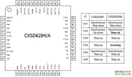
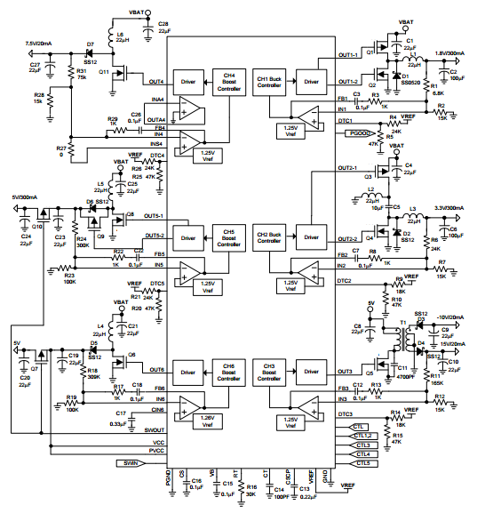
五,产品封装图 (Package)  六.电路原理图  七,功能概述 General The CXSD6284/A provides voltage-mode feedback con-trols for six DC/DC PWM converters (CH1 to CH6). Each channel operates with an error amplifier, PWM comparator,short-circuit comparator, ON/OFF control, and output driver. An internal temperature-compensated voltage pro-vides reference voltages for each channel. An triangular-wave oscillator(CT) with a timing resistor and capacitor generates triangular waves to each channel. A inverting amplifier(CH4) cooperates with the error amplifier for an inverting converter (with negative output voltage) . Reference Voltage The CXSD6284 outputs a temperature- compensated ref-erence voltage(2.49V) at VREF pin. It is regulated from the voltage at VCC pin and can source current of max.1mA to external loads. It also supplies bias for the IC’s internal circuitry. Triangular-wave Oscillator The triangular-wave oscillator is designed to generates a triangular oscillation signal (CT) with amplitude of 0.3V~0.8V at CT pin, providing signal to CH6. The oscilla-tor frequency is settable from 100kHz to 1MHz and set by a timing resistor and a timing capacitor connected re-spectively from RT and CT pins to ground. Additional two triangular oscillation signals (CT1 and CT2) are also in-ternally generated with amplitude of 1.1V~1.8V. The CT1 is in phase with the CT to the PWM comparators of CH2 and CH4; the CT2 is out of phase with the CT to the PWM comparators of CH1, CH3, and CH5. Error Amplifier The error amplifier is designed with unit-gain-bandwidth of 1MHz and to satisfy wide application requirements. It works with enternal resistor-capacitor network for each converter’s feedback compensation. The loop gain can be set by connecting a feedback resistor and capacitor from the output pin(FB) to inverted input pin of the error amplifier for stable operations. Inverting Amplifier (Inv Amp) The inverting amplifier detects the inverting DC/DC con-verter output voltage (as a negative voltage) and outputs a control signal to the error amp. 八,相关产品 更多同类产品......
发表评论
| |||||||||||||||||||||||||||||||||||||||||||||||||||||||||||||||||||||||||||||||||||||||||||||||||||||||||||||||||||||||||||||||||||||||||||||||||||||||||||||||||||||||||||||||||||||||||||||||||||||||||||||||||||||||||||||||||||||||||||||||||||||||||||||
发表时间:2020-04-22浏览次数:275
| 最新信息 |
|---|
| (1.)CXLE86296D 五通道高 ... (2.)CXLE86295D 五通道高 ... (3.)CXLE86294E PWM调光LE ... (4.)CXLE86293EI 线性恒流 ... (5.)CXLE86292CI 五通道I2 ... (6.)CXLE86291C 三通道PWM ... (7.)CXLE83205X PWM调光LE ... (8.)CXLE83204XS高精度PWM ... (9.)CXLE83203F:高功率DIP7 ... (10.)CXLE83202F:高精度PWM ... |
| 头条信息 |
|---|


