CXSU63140是一种固定开关频率(典型为1MHz)、电流模式、升压集成N沟道MOSFET的稳压器。该设备允许使用便携式设备用电感器和输出电容器。当前模式控制方案提供快速的瞬态响应和良好的输出电压精度欠压闭锁、限流、超温停堆-输出过载时的老化

-
[ 产品资料下载 ]
目录
1.产品概述 2.产品特点
3.应用范围 4.下载产品资料PDF文档
5.产品封装图 6.电路原理图
7.功能概述 8.相关产品
一,产品概述(General Description)
The CXSU63140 is a fixed switching frequency (1MHz typical), current-mode, step-up
regulator with an inte-grated N-channel MOSFET. The device allows the usage of small
inductors and output capacitors for portable devices. The current-mode control scheme
provides fast transient response and good output voltage accuracy.The CXSU63140 includes
under-voltage lockout, current-limit, and over-temperature shutdown preventing dam-
age in the event of an output overload
二.产品特点(Features)
1.)Wide 2.5V to 6V Input Voltage Range
2.)Built-in 0.6Ω N-Channel MOSFET
3.)Built-in Soft-Start
4.)High Efficiency up to 90%
5.)<1μA Quiescent Current During Shutdown
6.)Current-Mode Operation
Stable with Ceramic Output Capacitors
Fast Transient Response
7.)Current-Limit Protection
8.)Over-Temperature Protection with Hysteresis
9.)Available in a Tiny 5-Pin SOT-23 and TSOT-23Packages
10.)Lead Free and Green Devices Available(RoHS Compliant)
三,应用范围 (Applications)
Cell Phone and Smart Phone
PDA, PMP, MP3
Digital Camera
Boost Regulators
四.下载产品资料PDF文档
需要详细的PDF规格书请扫一扫微信联系我们,还可以获得免费样品以及技术支持!

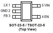
五,产品封装图 (Package)

|
PIN. |
FUNCTION |
|
|
NO |
NAME |
|
|
1 |
LX |
Switch pin. Connect this pin to inductor/diode here. |
|
2 |
GND |
Power and signal ground pin. |
|
3 |
FB |
Feedback Input. The device senses feedback voltage via FB and regulate the voltage at 1.23V. |
|
4 |
EN |
Enable Control Input. Forcing this pin above 1.0V enables the device. Forcing this pin below 0.4V to |
|
5 |
VIN |
Main Supply Pin. Must be closely decoupled to GND with a 2.2μF or greater ceramic capacitor. |
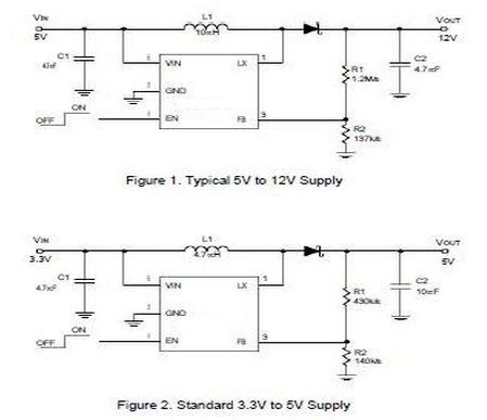
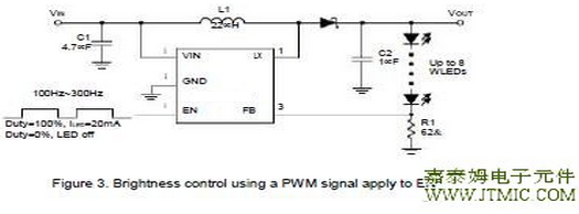
六.电路原理图


七,功能概述
Main Control Loop
The CXSU63140 is a constant frequency and current-mode switching regulator. In normal operation,
the internal N-channel power MOSFET is turned on each cycle when the oscillator sets an internal
RS latch, and then turned off when an internal comparator (ICMP) resets the latch. The peak inductor
current at which ICMP resets the RS latch is controlled by the voltage on the COMP node which is the
output of the error amplifier (EAMP). An external resis-tive divider connected between VOUT and
ground allows the EAMP to receive an output feedback voltage VFB at FB pin. When the load current
increases, it causes a slightly to decrease in VFB associated with the 1.23V reference,which in turn,
it causes the COMP voltage to increase until the average inductor current matches the new load current.
VIN Under-Voltage Lockout (UVLO)
The Under-Voltage Lockout (UVLO) circuit compares the input voltage at VIN with the UVLO threshold
to ensure the input voltage is high enough for reliable operation.The 100mV (typ) hysteresis prevents
supply transients from causing a restart. Once the input voltage exceeds the UVLO rising threshold,
startup begins. When the in-put voltage falls below the UVLO falling threshold, the controller turns
off the converter.
Soft-Start
The CXSU63140 has a built-in soft-start to control the output voltage rise during start-up. During
soft-start, an internal ramp voltage, connected to the one of the positive inputs of the error
amplifier, raises up to replace the reference voltage (1.23V typical) until the ramp voltage
reaches the reference voltage.
Current-Limit Protection
The CXSU63140 monitors the inductor current, flows through the N-channel MOSFET, and
limits the current peak at current-limit level to prevent loads and the CXSU63140 from
damaging during overload or short-circuit conditions.
Over-Temperature Protection (OTP)
The over-temperature circuit limits the junction tempera-ture of the CXSU63140. When
the junction temperature ex-ceeds 150 oC, a thermal sensor turns off the power MOSFET
allowing the devices to cool. The thermal sen-sor allows the converters to start a soft-start
process and regulates the output voltage again after the junction tem-perature cools by 40oC.
The OTP is designed with a 40oC hysteresis to lower the average Junction Temperature
(TJ) during continuous thermal overload conditions in-creasing the lifetime of the device.
Enable/Shutdown
Driving EN to the ground places the CXSU63140 in shut- down mode. When in shutdown,
the internal power MOSFET turns off, all internal circuitry shuts down, andthe quiescent
supply current reduces to 1μA maximum.
八,相关产品 更多同类产品......
|
Switching Regulator > Boost Converter |
|||||||||||
|
Part_No |
Package |
Archi-tecture |
Input Voltage |
Max Adj. Output Voltage |
Switch Current Limit (max) |
Fixed Output Voltage |
Switching Frequency |
Internal Power Switch |
Sync. Rectifier |
||
|
min |
max |
min |
max |
(A) |
(V) |
(kHz) |
|||||
|
SOT89 |
VM |
0.9 |
5.5 |
2.5 |
5.5 |
0.5 |
1.8|2.6|2.8|3 |3.3|3.8|4.5|5 |
- |
No |
Yes |
|
|
MSOP8|TSSOP8 |SOP8 |
VM |
2.5 |
5.5 |
2.5 |
- |
- |
- |
200 ~ 1000 |
No |
No |
|
|
TSSOP8|SOP-8P |
VM |
1 |
5.5 |
2.5 |
5 |
1 |
2.5|3.3 |
300 |
Yes |
Yes |
|
|
SOP8 |
CM |
3 |
40 |
1.25 |
40 |
1.5 |
- |
33 ~ 100 |
Yes |
No |
|
|
TQFN5x5-32 |
CM |
2.5 |
6.5 |
2.5 |
18 |
3 |
No |
1200 |
Yes |
No |
|
|
TSOT23-5 TDFN2x2-6 |
CM |
2.5 |
6 |
2.5 |
20 |
2 |
- |
1500 |
Yes |
No |
|
|
TQFN4x4-6 TDFN3x3-12 |
CM |
1.8 |
5.5 |
2.7 |
5.5 |
5 |
- |
1.2 |
Yes |
Yes |
|
|
SOT23-5 |
CM |
2.5 |
6 |
2.5 |
32 |
1 |
- |
1000 |
Yes |
No |
|
|
TSOT-23-6 TDFN2x2-8 |
CM |
1.2 |
5.5 |
1.8 |
5.5 |
1.2 |
- |
1.2 |
Yes |
Yes |
|
◀ 上一篇:固定1.2兆赫振荡器频率同步整流器CXSU63139低ESR输出电容稳定电流模式升压调节器92%效率
下一篇▶:自动进入脉冲频率调制PFM CXSU63141同步整流器固定开关频率1MHz电流模式升压调节器内同步整流器效率高达92%


