CXSD61051 The switching frequency is programmable from 100KHz to 500KHz and the synchronous architecture provides for highly efficient designs. Current mode operation provides fast transient response and eases loop stabilization
-
[ CXSD61051 ]
目录
1.产品概述 2.产品特点
3.应用范围 4.产品封装图
5.电路原理图 6.产品PCB
7.产品BOM 8.产品PDF文档
9.功能概述 10.相关产品
一,产品概述(General Description)
The CXSD61051 is a synchronous step down regulator with CC control from a high voltage input supply. Operating with an input voltage
range of 8V ~ 30V, the CXSD61051 achieves 3.5A continuous output current with excellent load and line regulation. The switching frequency is programmable from 100KHz to 500KHz and the synchronous architecture
provides for highly efficient designs. Current mode operation provides fast transient response and eases loop stabilization.
The CXSD61051 requires a minimum number of readily available standard external components. Other features include cable compensation programmable current limit and thermal shutdown.
The CXSD61051 converters are available in the industry standard SOP8-PP packages
二.产品特点(Features)
Wide Input Voltage Range: 8V ~ 30V
Up to 93% Efficiency
Programmable Switching Frequency up to 500KHz
No Loop Compensation Required
CC/CV control
Programmable CC Current
Thermal Shutdown
Available in SOP8-PP Package
三,应用范围 (Applications)
Car Charger / Adaptor
LED Driver
Pre-Regulator for Linear Regulators
Distributed Power Systems
Battery ChargerCar Charger / Adaptor
LED Driver
Pre-Regulator for Linear Regulators
Distributed Power Systems
Battery Charger
四,产品封装图 (Package)
|
PIN |
NAME |
DESCRIPTION |
|
1 |
FB |
Feedback |
|
2 |
ILIM |
CC Current Settng |
|
3 |
EN |
Enable |
|
4 |
PDRI |
PMOS Gate Drive |
|
5 |
NDRI |
NMOS Gate Drive |
|
6 |
VIN |
Input Supply Voltage |
|
7 |
RT |
Frequency setting |
|
8 |
SW |
Switch Node |
|
9 |
GND |
Ground |
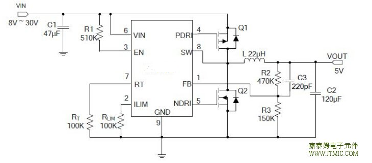
五,电路原理图
六, 产品PCB
(略)
七.产品BOM
(略)
八.产品PDF文档
需要详细的PDF规格书请扫一扫微信联系我们,还可以获得免费样品以及技术支持!

九,功能概述
Application Information
The CXSD61051 operates by a constant frequency, current mode architecture. The output voltage is set
by an external divider returned to the FB pin. An error amplifier compares the divided output voltage with
a reference voltage of 1.21V and adjusts the peak inductor current accordingly.
Thermal Protection
The total power dissipation in CXSD61051 is limited by a thermal protection circuit. When the device
temperature rises to approximately +160°C, this circuit turns off the output, allowing the IC to cool. The
thermal protection circuit can protect the device from being damaged by overheating in the event of fault
conditions. Continuously running the CXSD61051 into thermal shutdown degrades device reliability.
Current Limit
Current limit detection occurs during the off-time by monitoring the current through the low-side switch
using an external resistor, RLIM. The current limit value is defined by RLIM. If during the off-time the
current in the low-side switch exceeds the user defined current limit value, the next on-time cycle is
immediately terminated. Current sensing is achieved by comparing the voltage across the low side FET
with the voltage across the current limit set resistor RLIM. For example, the current limit value is 4.5A by
the RLIM =100K. The current limit value rises when the set resistor RLIM rises. The maximum output
current is set by RLIM: RLIM (kΩ) = 1500 · IMAX (A) / RDS_PMOS (mΩ).
Oscillator Frequency
The CXSD61051 oscillator frequency is set by a single external resistor connected between the RT pin and
the GND pin. The resistor should be located very close to the device and connected directly to the pins
of the IC (RT and GND). An internal amplifier holds the RT pin at a fixed voltage typically 0.6V. The
oscillator frequency rises when the resistor RT falls. To determine the timing resistance for a given
switching frequency, use the equation below:
RT(kΩ)= 22000 /fOSC(kHz)
Setting Output Voltage
The output voltage is set with a resistor divider from the output node to the FB pin. It is recommended to
use divider resistors with 1% tolerance or better. To improve efficiency at very light loads consider using
larger value resistors. If the values are too high the regulator is more susceptible to noise and voltage
errors from the FB input current are noticeable. For most applications, a resistor in the 10kΩ to 1MΩ
range is suggested for R3. R2 is then given by:
R2 = R3 · [(VOUT / VREF) – 1]
where VREF is 1.21V.
Output Cable Resistance Compensation
To compensate for resistive voltage drop across the charger's output cable, the CXSD61051 integrates a
simple, user-programmable cable voltage drop compensation using the impedance at the FB pin.
Choose the proper feedback resistance values for cable compensation refer to the curve in Figure 1.
The delta VOUT voltage rises when the feedback resistance R3 value rises, use the equation below
十,相关产品 更多同类产品......
|
高压同步DC-DC降压IC |
|||||||||
|
型号 |
输入耐压 |
输出电压 |
输出电流 |
反馈电压 |
工作频率 |
效率 |
静态工 作电流 |
待机电流 |
封装 |
|
8V-35V |
可调输出 带线损补偿 |
2A/带可调恒流设置 |
1.21V |
130K |
95% |
1.3mA |
112uA |
SOP-8 |
|
|
8V-35V |
可调输出/带线损 补偿带使能端 |
2A/带可调恒流设置 |
1.21V |
130K |
93% |
1.3mA |
SOP-8 |
||
|
4.5-20V |
可调输出 |
2.0A |
0.923V |
340K |
95% |
1mA |
6uA |
SOP-8 |
|
|
4.5-27V |
可调输出 |
2.0A/2.5A |
0.925V |
340K |
96% |
1.3mA |
0.3uA |
SOP-8 |
|
|
8V--35V |
可调输出 带线损补偿 |
2.0A/带可调限流保护 |
1.2V |
100-500K |
93% |
750uA |
110uA |
ESOP-8 |
|
|
10V--35V |
可调输出 带线损补偿 |
2.5A/带可调限流保护 |
1.2V |
100-500K可调 |
93% |
15mA |
110uA |
SOP-8 |
|
|
8V-35V |
可调输出 带线损补偿 |
2.8A/带可调限流保护 |
1.21V |
100-500K可调 |
93% |
15mA |
110uA |
SOP-8 |
|
|
8V-35V |
可调输出 带线损补偿 |
3.2A/带可调限流保护 |
1.21V |
100-500K可调 |
93% |
15mA |
110uA |
SOP-8 |
|
|
4.6-22V |
可调输出 |
3.0A |
0.923V |
340K |
95% |
55uA |
1uA |
ESOP8 |
|
|
4.5-27V |
可调输出 |
3.0A |
0.925V |
340K |
93% |
1.3mA |
0.3uA |
ESOP8 |
|
|
4.5V-23V |
可调输出 |
3.5A |
0.925V |
340K |
96% |
2.5mA |
ESOP-8 |
||
|
8V-35V |
可调输出 带线损补偿 |
扩流4.5A带 可调限流保护 |
1.21V |
100-500K可调 |
95% |
14mA |
100uA |
ESOP8 |
|
|
3.6-40V |
可调输出 |
2.0A |
0.8V |
440K |
94% |
74uA |
0.07uA |
ESOP-8 |
|
|
4.5-20V |
可调输出 |
4.0A |
0.923V |
340K |
95% |
1.6mA |
6uA |
ESOP8 |
|
|
3.5-23V |
可调输出 |
2.0A |
0.6V |
600K |
96% |
400uA |
1uA |
SOT-26 |
|
|
4.5-17V |
可调输出 |
2.0A |
0.6V |
600K |
96% |
400uA |
1uA |
SOT-26 |
|
|
4.5V-23V |
可调输出 |
2.0A |
0.8V |
600K |
92% |
800uA |
SOT-26 |
||
|
3.3-17V |
可调输出 |
2.0A |
0.6V |
600K |
96% |
400uA |
4uA |
SOT-26 |
|
|
4.5-26V |
可调输出 |
1.2A |
0.8V |
1.4M |
94% |
600uA |
1uA |
SOT-26 |
|
|
4.0-42V |
可调输出 |
1.5A |
0.8V |
650K |
91% |
600uA |
6uA |
SOT-26 |
|


