|
CXSD6289两个同步降压型脉宽调制控制器脉冲宽度调制控制器设计用于同步驱动两个N通道mosfet buck拓扑 | ||||||||||||||||||||||||||||||||||||||||||||||||||||||||||||||||||||||||||||||||||||||||||||||||||||||||||||||||||||||||||||||||||||||||||||||||||||||||||||||||||||||||||||||||||||||||||||||||||||||||||||||||||||||
|
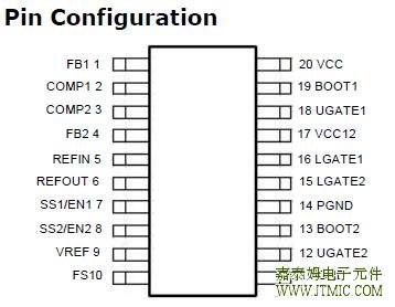
目录 1.产品概述 2.产品特点 一,产品概述(General Description) The CXSD6289 has two synchronous buck PWM control-lers with high 1.)Two Synchronous Buck Converters(OUT1,OUT2) Graphic Cards 需要详细的PDF规格书请扫一扫微信联系我们,还可以获得免费样品以及技术支持! 五,产品封装图 (Package) 六.电路原理图
Output Inductor Selection (Cont.) select the capacitor voltage rating to be at least 1.3 times higher than the maximum input voltage. During power up, the input capacitors have to handle large amount of surge current. If tantalum capacitors are used, make sure they are surge tested by the manufactures. If in doubt, consult the capacitors manufacturer. For high frequency decoupling, a ceramic capacitor 1uF can be connected between the drain of upper MOSFET and the source of lower MOSFET. capacitance (CRSS) and maximum output current requirement. The losses in the MOSFETs have two components: conduction loss and transition loss. For the upper and lower MOSFET, the losses are approximately given by the following : frequency St is the switching interval sw D is the duty cycle Note that both MOSFETs have conduction losses while the upper MOSFET include an additional transition loss.The switching internal, tsw, is a function of the reverse transfer capacitance CRSS. The (1+TC) term is to factor in the temperature depen-dency of the RDS(ON) and can be extracted from the “RDS(ON) performance, since many factors can affect how well it works. Therefore, the limitations and suggestions of this method must be pro-vided for users to understand how to work it well.The short circuit protection was not designed to work for the output in initial short condition. In this case, the short circuit protection may not work, and damage the MOSFETs. If the circuit still works, remove the short can cause an inductive kick on the phase pin, and it may damage the IC and MOSFETs. If the resistance of the short is not low enough to cause protection, the regulator will work as the load has Short Circuit Protection (Cont.) should include wiring, PCB traces, contact resistances, and all of the return paths.The higher duty cycle will give a higher COMP voltage level, and it is easy to touch the trip point. The compensa- if the cur-rent rises too fast, it may cause a false trip. The output capacitance and its ESR can affect the rising time of the current during short. 八,相关产品 更多同类产品......
发表评论
| ||||||||||||||||||||||||||||||||||||||||||||||||||||||||||||||||||||||||||||||||||||||||||||||||||||||||||||||||||||||||||||||||||||||||||||||||||||||||||||||||||||||||||||||||||||||||||||||||||||||||||||||||||||||
发表时间:2020-04-22浏览次数:289


| 最新信息 |
|---|
| (1.)CXLE86296D 五通道高 ... (2.)CXLE86295D 五通道高 ... (3.)CXLE86294E PWM调光LE ... (4.)CXLE86293EI 线性恒流 ... (5.)CXLE86292CI 五通道I2 ... (6.)CXLE86291C 三通道PWM ... (7.)CXLE83205X PWM调光LE ... (8.)CXLE83204XS高精度PWM ... (9.)CXLE83203F:高功率DIP7 ... (10.)CXLE83202F:高精度PWM ... |
| 头条信息 |
|---|

